Before we go deeper into the various component families, we need to clarify the component lead forms of today’s component packaging technology and what is going to be eventually phased out and what is new and why.
The pin (component lead) pitch and the overall body height are continually shrinking. This is why the SSOP and TSOP land pattern names have to be dropped from the standard. S = Shrink for Fine Pitch and T = Thin for low profile height. If these 2 values are constantly changing then where is the line drawn? Whose part is Thin or Fine Pitch and by what measure? The Gull Wing lead has hit the wall at 0.4 mm pitch. Most assembly shops will try to convince you to swap that part out of your design for a larger pin pitch however, No-lead SON and QFN lead styles are being produced and manufactured at 0.4 mm pitch with no problems. The finer pitch parts have more I/O’s and a smaller footprint with a much lower profile than J-Lead or Gull Wing packages, so it’s obvious that the component industry is going to be no-lead or bottom only flat lead or side lead packages.
Let’s review the existing component lead forms in alphabetical order. The BGA or Ball Grid Array has been around since the 1980’s but the pin pitch started out with 1.5 mm and then quickly went to 1.27 mm (50 mils) for about 15 years. Then in the late 1990’s, the 1 mm pitch BGA was introduced and every couple years a smaller pin pitch was introduced. Today 0.4 mm pitch BGA’s are in every cell phone and 0.3 mm pitch BGA’s are the next generation.
There are 2 types of BGA Ball Leads –
- Collapsing – this is normally 0.65 mm pitch and higher, where the Land (pad) is smaller than the Ball size to allow the Ball to collapse around the sides of the Land. This requires a non-solder mask defined Land where the solder mask must be larger than the Land.
- Non-collapsing – this is normally 0.5 mm pitch and smaller, where the Land (pad) is larger than the ball to allow for via-in-pad technology and provide an adequate annular ring. The solder mask can be the same size as the Land. In some cases the Land for fine pitch BGA’s is solder mask defined where the solder mask encroaches slightly over the land. This provides protection for any trace routing between the lands but the most significant benefit is to help secure the Land to the PCB. During cell phone “drop testing”, the BGA solder joint normally holds better than the land to the Prepreg. i.e.: drop tests prove that the non-solder mask land will rip from the PCB before the solder joint breaks. So the solder mask defined land is secured better to the PCB for drop testing.
For more information about BGA’s, read my white paper “Metric Pitch BGA and Micro BGA Routing Solutions”.

Ball Lead

Non-collapsing Ball vs: Collapsing Ball
While we’re on the subject of “Grid Array Lead Forms” let’s move on down the list of bottom only lead types. The next lead form in the “bottom only” category is the “Bump” lead. This is widely used in a package called “Land Grid Array” or LGA. The Land (pad) size can be the same as the Bump diameter and via-in-pad can be much more forgiving than BGA voids due to a dimple in the Land after the plug and plate process. This lead form is also highly lead-free compatible.

Bump Lead
The next Grid Array lead form is the “Bottom Flat” and is also used in Land Grid Array (LGA) component packages. Linear Technologies is the leading provider of Bottom Flat Lead LGA packages. This lead form is also highly compatible with lead-free solder alloys as there is no reason for wetting (flow) properties in the solder.
We can also categorize the Pull-back Lead SON and QFN component packages with this solder joint goal as a slight periphery land is required to allow the solder to move from under the lead to the periphery to surround the protruding lead for a solid solder joint.

Bottom Flat Lead
The next Grid Array component lead is the “Column”. Actel and Xilinx are the leading manufacturers for this lead style. You will not find any pin pitches smaller than 1 mm for the Column Lead. The Land must be slightly larger than the column to form a good solder joint.

Column Lead
Column Lead Solder Joint.

Column Lead Solder Joint
The last SMT Grid Array is the newest lead form in the industry is the “Pillar Column”. Recently introduced by Actel, this component lead has much promise for an improved solder joint. But time will tell how long this one will last.

Pillar Column Lead
Here is a solder joint for the Pillar Column Lead. Nice connection!

Pillar Column Lead Solder Joint
The “Corner Concave” lead form is primarily used for the Oscillator component family. It’s perfect for Oscillators because it only has 4 leads that are necessary for the standard Oscillator requirements.

Corner Concave Lead

Cylindrical End Cap Lead
“Flat Lead” components are coming on strong. These are the SODFL (Small Outline Diode Flat Lead) 2 leaded components and the SOTFL (Small Outline Transistor Flat Lead) packages that come in 3, 5, 6 and 8 lead components. Both of these component families are the direct replacement for the Gull Wing Lead SOD and SOT-23 packages.

Flat Lead
“Flat No-lead” is used in the SON (Small Outline No-lead) with terminals on 2 sides and QFN (Quad Flat No-lead) with leads on 4 sides. The most common SON & QFN today is the “Edge” lead, where the component lead starts under the component and goes out to the component body edge. This solder joint goal requires a Toe, Heel and Side solder fillet where the toe joint is visible for inspection.

Flat No-lead Edge
The other Flat No-lead is referred to as a “Pull-back” lead or “Bottom Only”. The solder joint goal is a periphery land around the terminal. Pull-back leads come in 2 lead shapes –
- D-Shape or Bullet in some CAD tools
- Rectangle
This lead style has the same solder joint goals as the Bottom Only LGA lead.

Bottom Only Lead
The “Flat Thermal” lead comes in a DPAK where the signal pins and Gull Wing and the thermal lead is Flat. The “Flat Thermal” lead is also used as the heat sink for SON, QFN, SOP and QFP packages. It is usually embedded in the plastic component body and therefore the solder joint goals are usually 1:1 scale for the maximum component lead size and Land size.

Flat Bottom Only Lead
Every PCB designer is familiar with the Gull Wing lead, but it has 2 separate rule sets that are defined by the pin pitch –
- Less than 0.625 mm pitch
- Greater than 0.625 mm pitch
We need to note that 70% of the solder strength in the Gull Wing lead is in the “Heel” joint.

Gull Wing Lead

Gull Wing Solder Joint
The “Inward Flat Ribbon L” is used for the Molded Body component family. This includes Polarized and Non-polarized Capacitors, Inductors, Resistors and LED’s. The most popular is the Tantalum Capacitor.

Inward Flat Ribbon L Lead
The “J-Lead” is one of the original SMT leads that became popular with the PLCC (Plastic Leaded Chip Carrier) and then the SOJ (Small Outline J-Lead). This lead form was very popular because the leads were stable and easy to manually solder. And the solder joint was easy to inspect. However, with the advent of High Speed technology, lead-free solder, low profile fine pitch component packages, this lead form will be one of the first SMT leads to become obsolete.

J-Lead

J-Lead Solder Joint
The “Outward Flat Ribbon L” lead is used to reduce the footprint size of SOT and SOP components. It’s similar to a Gull Wing lead, but the lead bends downward immediately coming out of the component body and then is bent flat. The flat lead is very compatible to lead-free solder alloys and takes up less PCB real-estate. Since there is no heel and these components are so “low profile”, the land is usually trimmed at the nominal component body. If the land (pad) protrudes under the component body, it will end up with solder on the bottom of the component during reflow.
The Outward L lead also has 2 separate rule sets that are defined by the pin pitch –
- Less than 0.625 mm pitch
- Greater than 0.625 mm pitch

Outward L Lead
The first component lead was the Plated Through-hole (PTH) and it’s still used today for almost every type of discrete component and connector. The through-hole components are mostly used for today’s power supply boards and proto-type boards that require hand soldering and rework.

Plated Though-hole Lead
The “Rectangular End Cap” is used for discrete resistors, capacitors and inductors. This lead type is by far the most popular due to the component count. An average PCB has 80 – 90% of the total part quantity using the Rectangular End Cap lead form. These components are easy to manually solder and easy to rework if necessary. However, the new DFN (Dual Flat No-lead) component with Bottom Only terminations is better for lead-free solder and part placement density.

Rectangular End Cap Lead
Here is a rectangular end cap solder joint.

Rectangular End Cap Solder Joint
The “Side Lead” comes in 3 different lead styles –
- Concave
- Convex
- Flat
The Side Lead is on the outside perimeter of the component body and normally runs from the bottom to the top of the component. It is used widely for Chip Array’s and LCC (Leadless Chip Carriers) and has 2 different sets of solder joint goals depending on the lead pitch –
- Pitch is less than or equal to 1 mm
- Pitch is greater than 1 mm
Here is the Concave “Side Lead” –

Concave Lead
Here is the Flat “Side Lead” –

Side Flat Lead
Here is the Convex “Side Lead” –

Side Convex Lead
The last component lead form in the list is the “Under Body Outward L”. This lead form is used for Aluminum Electrolytic Capacitors and 2-pin SMT Crystals. This lead form has 2 different solder joint goals that are based on the component height. Once the component height exceeds 10 mm, the solder joint goals have to be more robust.

Under Body Outward L Lead
Now that we covered all the component lead forms, we can dive into the various component families and relate their lead forms back to this post. It’s going to be interesting to find out what new component lead will be invented by a component manufacturer in the years to come, but when they do, the IPC-7351 land pattern committee will be there to develop the optimized solder joint goal chart.
Next week I’m planning on posting “The Anatomy of a Land Pattern” and all the various elements that a quality land pattern must have in order to qualify for PCB design perfection. Here is a sample picture of the details we’ll cover –
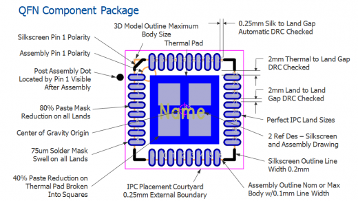
Anatomy of a Land Pattern